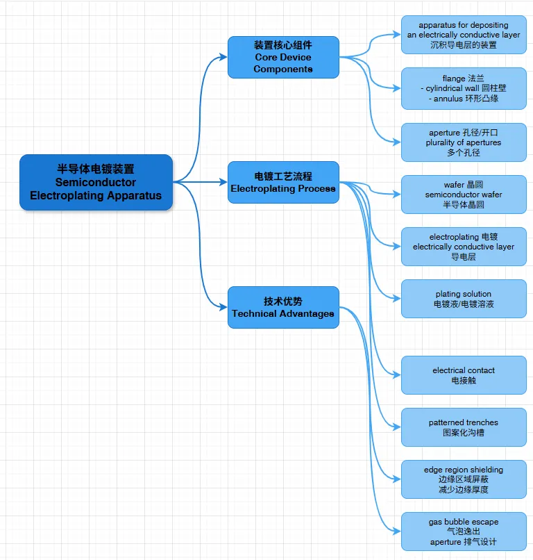
An apparatus for depositing an electrically conductive layer on the surface of a wafer comprises a flange.
The flange has a cylindrical wall and an annulus attached to a first end of the cylindrical wall.
The annulus shields the edge region of the wafer surface during electroplating, reducing the thickness of the deposited electrically conductive layer on the edge region.
Further, the cylindrical wall of the flange can be provided with a plurality of apertures adjacent the wafer, allowing gas bubbles entrapped on the wafer surface to readily escape.
The manufacture of semiconductor devices often requires the formation of electrical conductors on semiconductor wafers.
For example, electrically conductive leads on the wafer are often formed by electroplating (depositing) an electrically conductive layer such as copper on the wafer and into patterned trenches.
Electroplating involves making electrical contact with the wafer surface upon which the electrically conductive layer is to be deposited (hereinafter the "wafer plating surface").
Current is then passed through a plating solution
| apparatus for depositing an electrically conductive layer | ||
| flange with cylindrical wall and annulus | ||
| electroplating | ||
| wafer | ||
| aperture |

